Project title in Latvian: Topoloģiskie pusmetāli energoefektīvai elektronikai
Project title in English: Topological semimetals towards low-dissipation electronics
Project number: lzp-2021/1-0302
Project implementer: University of Latvia (UL)
Partners of the project: Institute of Solid State Physics, University of Latvia (ISSP, UL)
Project coordinator: Gunta Kunakova
The leading structural unit of the project implementation at the University of Latvia is the Faculty of Science and Technology, Institute of Chemical Physics
Project implementation period: 03.01.2022. – 30.12.2024.
Total budget: 304 099,70 EUR, including funding allocated to the LU part of the project: EUR 223 099,70
Abstract
Two-dimensional layered crystals of transitional metal dichalcogenides (TMDs) have recently emerged as an important quantum materials for energy harvesting applications and in information technology. Recent discoveries of non-trivial phases, such as the 2D topological insulator and quantum spin-hall insulating phase in monolayers, and type-II Weyl semimetal phase in multi-layer TMD crystals have led to intense research of growth and handling of TMDs. Currently vast majority of fundamental research in detecting and manipulating nontrivial properties of TMDs has been conducted in samples fabricated from mechanically exfoliated and stacked flakes with other 2D materials, such as hexagonal boron nitride (hBN). This approach is valid for proof-of concept demonstrations, but it leads to large device – to – device variations and is not suitable for development towards practical applications. The aim of this proposal is to achieve well defined, reproducible, and topologically protected charge transport on the edge in state-of-the-art topological TMD thin film materials towards low dissipation and topologically protected electronics, and for fundamental studies of Majorana and Weyl fermions. Fabricated heterostructures will be integrated in nanodevices for charge transport characterization particularly focusing on fundamental studies of exotic topological edge state transport.
Project team:
University of Latvia
- Leading researcher / principal investigator– Gunta Kunakova;
- Leading researcher – Jānis Švirksts;
- Leading guest researcher – Nataliya Amirulloeva (SHEI Prydniprovska State Academy of Civil Engineering and Architecture, Dnipro, Ukraine);
- Researcher (student) – Andrejs Terehovs;
- Researcher (student) – Jelena Sušinska;
- Researcher (student) – Darja Dolbe;
- Researcher (student) – Āris Jansons;
Researcher (student) – Emmanuel Jose.
Institute of Solid State Physics, University of Latvia (ISSP, UL)
- Leading researcher – Gatis Mozoļevskis
- Researcher (student) – Helēna Ose
- Researcher (student) – Aleksejs Bendins
- Researcher (student) – Edvīns Ļetko
Progress of the project:
In the first quarter of the project, work was carried out in the research activity <WP1> "WTe2 growth". To develop growth methods of high-quality WTe2/hBN heterostructures, effort was focused on the following tasks: 1) setting up the equipment. Even though the University of Latvia, Institute of Chemical Physics (hereinafter UL-ICP) has all the necessary infrastructure for growth of WTe2 by the Chemical Vapor Deposition (CVD), it was decided to install a setup designated for these specific syntheses. 2) To select the most suitable growth strategies.
In the project activity <WP1> it was initially planned to develop two CVD approaches - a) from WTe2 and b) WCl6/W(CO)6 /Te precursors. However, the mentioned precursors oxidize rapidly / are unstable under ambient conditions hence WO3/NaCl was chosen for the initial syntheses. 3) Determination of the “growth parameter window” for obtaining WTe2, initially using Si/SiO2 substrates.
The project's team was joined by two students in the B.Sc. and M.Sc. programs "Chemistry".
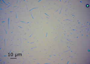
To determine the growth parameters of WTe2 structures, sequential syntheses were carried out using Si/SiO2 substrates. Some of the parameters needed to be fine-tuned to ensure growth of WTe2 are the following – temperature of the precursors and substrates, the heating rate, pressure, Ar/H2 ratio, duration of H2 gas flow, reaction time, precursor composition. For some of the parameters, initial values were taken from the literature as fixed while the others were determined by performing sequential syntheses. It has been determined that one of the most important factors is the “synthesis geometry”, that is, the sample and precursor arrangement in the furnace. In one of such test syntheses for establishing the most optimal geometry (Si/SiO2 substrates placed in the quartz boat together with the precursor), along with the formed coating of various droplet-like-structures, nanowires were obtained (see optical microscope image) containing W and weak signal of Te (EDX data). WTe2 nanowires and nanoribbons with their well-defined geometry are promising for further fundamental studies of exotic charge transport via “edge-state”, however their growth methods are far less explored compared to the synthesis of WTe2 crystals and thin films.
Along with the research within the activities <WP1> “WTe2 growth” and <WP2> “Structural characterization” student training to work with the Scanning Electron Microscopy (SEM), Atomic Force Microscopy (AFM), as well as with the tools in the cleanroom (ISSP, UL) was carried out.
Development of the WTe2 synthesis methodology has been continued conducting research in the project activities <WP1> (growth) and <WP2> (characterisation), in agreement with the initially planned time diagram. Research has been focused on the three main directions:
1) Growth of the WTe2 thin film / thin layer structures on Si/SiO2 to determine the “growth parameter window”. So far, non-homogenous coatings, several hundreds of micrometers large or, on the contrary, nanosized crystals in the centre of the droplets, as well as droplet-like structures, have been obtained. Stoichiometry studies using Energy Dispersive X-Ray spectroscopy (EDX) in the SEM indicate that the large crystals consist mostly of W (Te signals are not detected), while the fine ones are composed of W:Te (see the picture below).
WTe2 nanostructures on Si/SiO2, EDX mapping in the scanning electron microscope (A. Terehovs, batch 02.08.2022). The scale in the SEM image on the left is the same as for the element mapping in the center – 1 mm.
XPS spectra (ISSP, UL) were also taken for these samples, confirming the presence of non-stoichiometric WTe2, mostly oxidized.
2) Synthesis of WTe2 nanowires. Along with the research conducted to establish growth parameters of WTe2 thin films/thin structures, methodology for the synthesis of nanowires has also been developed. Compared to the WTe2/hBN structures, nanowires and nanoribbons can be easily transferred to other desired substrates, and their geometrical shape is particularly suitable for studies of fundamental charge carrier transport properties.
3) Synthesis of WTe2 thin films from pre-deposited WOx. In alternative to the complex multi-parameter synthesis thin WTe2 structures from W: and Te precursor, WTe2 films could be obtained by heating a sputtered layer of oxidized W in a Te environment. WOx films with a thickness of 15 – 30 nm on Si/SiO2 substrates were made at the partner's institution.
PhD student, initially included in the Projects scientific team will not be able to join; to strengthen the project’s implementation, vacancy for a research assistant / doctoral student was published in the local work advertisement domain https://cv.lv/lv/vacancy/868990/latvijas-universitate-lu/phd-position-in-the-field-of-experimental-condensed-matter-physics (deadline 05.09.2022), and in the Euraxess Research Assistant/Doctoral Student: 2D Transition Metal Dichalcogenide topological insulators (deadline 01.09.2022). After the evaluation procedure and interviews, the best candidate (from the Indian Institute of Science, Bangalore, India) has started the educational document evaluation procedure.
At the end of the quarter, the activities within the framework of the project were presented at the annual European Night of Research, which took place in the Academic Center of Natural Sciences, UL.https://www.lu.lv/notikumi/diena/notikums/e/zinatnieku-nakts-6/ . http://foto.lu.lv/arhiivs/2022/i_sep/30b/slides/ZN_031.html http://foto.lu.lv/arhiivs/2022/i_sep/30b/slides/ZN_051.html
. The scale in the SEM image on the left is the same as for the element mapping in the center – 1 mm.")

To improve the stoichiometry of WTe2 thin crystals obtained in the previous quarter as well as to fabricate thin-film-structures, elaborate work has been continued. In one of the syntheses, thin-layer structures and ribbon-like crystals were obtained (see optical microscope images on the right).
EDX/SEM as well as XPS analyses have been performed on these fabricated samples, confirming high quality, stoichiometric WTe2. Using determined growth parameters, impact of the “reaction time” and the substrate /precursor temperature have been studied further, aiming to obtain few/mono-layer structures or crystals in a controlled and reproducible manner. Taking the determined synthesis parameters for obtaining the stoichiometric WTe2 on Si/SiO2, growth on Si/SiO2/hBN substrates has been performed.
In addition to the growth of WTe2 crystals and few-layer on Si/SiO2 and Si/SiO2/hBN substrates, work on the synthesis and characterization of WTe2 nanowires has been continued. The results on developing the nanowire synthesis strategies is planned to be included in the course work (Master's study program, 2nd year student J. Sušinska).
Regardless the fact that candidate with a suitable profile and experience for implementing the project has been successfully found after posting the job advertisements, the visa procedure will take several months. To improve the implementation of the planned research activities and to support Ukrainian researchers, it is planned to employ another senior researcher Assoc. prof. N. Amirulloieva, from SHEI Prydniprovska State Academy of Civil Engineering and Architecture, Dnipro, Ukraine.
Recent call of support by the Latvian Council of Science allows to employ Ukrainian researcher in the ongoing projects https://www.lzp.gov.lv/lv/jaunums/par-ukrainas-petnieku-iesaisti-fundamentalo-un-lietisko-petijumu-projektos , and in agreement with the submission / evaluation procedure, support of 4100EUR was granted to employ Assoc. prof. N. Amirulloieva in the project over the period of 02.11. – 31.12.2022, for conducting additional research:
1.1. To conduct a literature study focusing on obtaining 2D materials (TMDs) by electrochemical methods.
1.2. To obtain stoichiometric WTe2 from the pre-deposited WO3 layers: to determine the synthesis parameters, and to summarize the obtained results.
1.3. To characterise the fabricated samples using Scanning Electron Microscopy and EDX.
At the end of the quarter of the project, all the planned additional studies were accomplished and literature review for obtaining 2D transition metal chalcogenides by electrochemical methods was completed.
The second year and the fifth quarter of the project has been started with an intensive work in all four research activities of the project - <WP1> “WTe2 growth”, <WP2> “Structural characterization”, <WP3> “Nanodevices” and <WP4> “Studies of transport via the edge states”:
- Growth of the WTe2 thin film / thin layer structures on hBN. Using the determined growth parameters and "synthesis geometry" for obtaining stoichiometric WTe2 structures on Si/SiO2 substrates, syntheses for the fabrication of heterostructures were performed: 1.1) vertical heterostructures with h-BN. Si/SiO2 chips coated with monolayer of h-BN were used as substrates. Compared to the growth on SiO2, the obtained WTe2 structure density per area is considerably less, but the ribbon-like WTe2 crystals can be still grown Si/SiO2/hBN substrates. More work will be done to improve the yield. 1.2) Lateral heterostructures. Flakes of hBN were transferred to Si/SiO2 substrates, and synthesis of WTe2 was performed: preliminary results indicate formation of the lateral heterostructures. Additional effort will be spent to determine the structural properties of the interface.
- Synthesis of WTe2 nanowires. During the fifth quarter of the project, the course work on the synthesis of WTe2 nanowires in terms of the Master’s study program "Chemistry", was submitted and defended, and experimental work on the Master's thesis was started. To obtain WTe2 nanowires, several methods of nanowire synthesis (on Si and SiO2 substrates, with and without Na doping) will be investigated, using conversion of free-standing WOx nanowires. The fabricated nanowires have been transferred onto a flat substrate, and integrated into devices for charge carrier transport measurements, this research is ongoing, and will be continued.
- Synthesis of WTe2 thin films from pre-deposited WOx. The parameters developed by the Ukrainian researcher recruited in the previous quarter, are further advanced to grow thin films with an improved crystallinity. Assoc. prof. N. Amirulloieva has successfully joined the project's research group. Charge carrier transport measurements were performed on some of these prepared thin film samples, showing highly metallic behaviour. During the synthesis of WTe2 films, some unexpected parameters were found favourable to formation of WTe2 nanoribbons.
During the sixth quarter, drafts of manuscripts for 3 potential publications are being prepared. So far, in terms of the project research activities, high-quality, stoichiometric WTe2 structures of different geometries on Si/SiO2 substrates, as well as heterostructures with hBN, WTe2 thin films and WTe2 nanowires are fabricated. Master's thesis (Chemistry) was defended on 08.06.2023 - J. Sušinska, "Synthesis and characterization of tungsten telluride nanowires".
The results achieved in the project so far were presented this quarter at 4 conferences (local and international):
- J. Sušinska, G. Kunakova. Synthesis of tungsten ditelluride nanostructures, 81st International Scientific Conference of the University of Latvia, Section “Nanotechnologies and Radiation Processes”, April 5, 2023, Riga, Latvia, oral.
- Terehovs, A. Šarakovskis, G. Kunakova. CVD growth of WTe2 monolayers on insulating substrates. 81st International Scientific Conference of the University of Latvia, Section “Nanotechnologies and Radiation Processes”, April 5, 2023, Riga, Latvia, oral.
- J. Sušinska, G. Kunakova. Growth and characterisation of WOx and WTe2 nanowires. NanoOstrava 2023, 15-18 May 2023, Ostrava, Czech Republic, poster.
- N. Amirulloieva, G. Mozolevskis, G. Kunakova. Synthesis and charge transport characterisation of WTe2 thin films. International Conference of Students and Young Scientists in Theoretical and Experimental Physics, HEUREKA-2023, May 16-18, 2023, Lviv, Ukraine (held online).
Two new students have started working in the project. Ā Jansons (PhD study program "Chemistry") has started work in the project activity <WP3> (nanodevices), focusing on development of encapsulation strategies of thin WTe2 structures and their heterostructures with hBN. D. Dolbe (Bachelor's study program "Chemistry") has started work in the activity <WP2> (characterization of the obtained structures), where it is planned to perform AFM measurements of WTe2 structures of different thicknesses (aiming to calibrate the structure contrast in the optical images with the actual thicknesses).
In this quarter, work on developing the methodology for synthesizing few-layer WTe2 structures and their heterostructures with h-BN has continued. New samples were synthesized for spectroscopic measurements (Raman and XPS, ISSP), which are necessary for confirming the structure. Additionally, WTe2/SiO2 samples were fabricated for developing encapsulation methodologies. Efforts to establish growth approaches for obtaining WTe2 nanowires and nanoribbons (both with and without Na) have also continued. The synthesized structures, obtained using various growth methods, were transferred to marked SiO2 substrates, and contacts were fabricated using EBL (ISSP). The fabricated samples were measured at room and low temperatures, and the charge transport properties (conductivity), and contact resistances were determined for individual nanowires.
On 29.09., the Researchers’ Night event took place at the University of Latvia, House of Natural sciences. J.Sušinska, A.Terehovs and D.Dolbe actively participated, presenting the results obtained in the project. In the picture, J.Sušinska presents nanowire synthesis methods and their integration into devices.

In the reporting quarter, reviews were received for the article submitted in June on WTe2 nanoribbons, and work on revising the article has begun. The revision requires HR-TEM and additional magnetotransport data.
During this period, J.Sušinska successfully completed training for EBL in the clean room (ISSP). Research has actively continued in all the planned work packages, including the growth of various WTe2 structures (2D materials, nanowires, heterostructures, thin films, structures from pre-patterned WO3 thin films), development of their encapsulation strategy, fabrication of nanodevices (using EBL and related equipment, ISSP), and characterization of the synthesized structures (Raman (ISSP), AFM, SEM-EDX). Magnetotransport measurements were performed in the 300-2K temperature range to determine the charge carrier properties of WTe2/SiO2 nanodevices. The data obtained show that the structures exhibit semiconductor characteristics, contrary to the expected metallic behaviour, suggesting that the material has degraded due to environmental exposure. To study and isolate new properties successfully, WTe2 needs to be encapsulated to protect it from oxygen and humidity.
Starting the final year of the project, work on revising the manuscript on WTe2 nanoribbons has continued, with efforts to perform additional HR-TEM measurements. Studies for obtaining atomically thin and few-layer WTe2 structures by CVD were also continued, and the manuscript draft on 2D WTe2/h-BN heterostructures was updated with the latest results, including growth reproducibility, distribution gradient of the obtained structures on the substrates, and evaluation of synthesis parameters such as reaction temperature, H2 flow, and growth time.
A draft of the manuscript on WTe2 nanowires and nanoribbons, obtained from WO3 nanostructures, was updated with the charge transport data. Work on encapsulation coatings were also continued, with the development of two encapsulation strategies - using polysilazane and hexylamine. The obtained coatings were studied by Raman spectroscopy, and the data were summarized for the manuscript draft.
In parallel with these studies, a development of methodology for estimating the thickness of WTe2 2D structures on SiO2 using optical contrast analysis has started.
At the end of March, a visit was made to Kaunas University of Technology in Lithuania, where contacts for WTe2 nanowires were fabricated using EBL.
To obtain lateral heterostructures with h-BN, efforts have continued to develop a methodology for etching h-BN monolayer coatings on SiO2. Additionally, work has progressed on several manuscript drafts, with ongoing measurements to support them, starting from AFM, SEM, optical microscopy, and spectroscopy data (XPS, FTIR, Raman), as well as device fabrication and magnetotransport measurements at cryogenic temperatures. Regarding the WTe2 nanoribbons, high-quality HR-TEM data have been obtained, which can be used to determine their growth direction. Furthermore, new samples have been fabricated, including nanowires and nanoribbons, WTe2 and WTe2/h-BN structures encapsulated using various methods, along with devices for magnetotransport measurements. Versatile charge carrier transport measurements have been conducted, and the resulting data have been processed and evaluated. In early June, A. Terehovs successfully defended his bachelor's thesis on the growth of WTe2/h-BN heterostructures by CVD and plans to continue his studies in the master’s program (Chemistry).
During this quarter, an additional function was installed on the PPMS cryostat – a horizontal sample rotator, which allows the sample to be rotated for angle-dependent magnetotransport measurements. The following measurements were performed on the fabricated WTe2 2D material samples at a temperature of 2K, where negative magnetoresistance was observed at certain angles, confirming the anisotropic properties of WTe2. These obtained results have been summarized and added to the manuscript draft. Meanwhile, work continued on supporting drafts of other manuscripts and performing measurements to complete missing data (additional Raman, XPS, AFM, and magnetotransport). In August and September, international conferences were attended, where the data obtained in the project were presented:
A. Terehovs, A. Jansons, A. Spustaka, G. Kunakova. Magnetotransport Studies of CVD Synthesized Tungsten Ditelluride 2D Crystals. Advanced Materials and Technologies, 26th International Conference, 26 – 30 August, 2024, Palanga, Lithuania, poster.
D. Dolbe, A. Terehovs, M. Zubkins, G. Mozolevskis, G. Kunakova. Site Selective Growth of 2D Tungsten Ditelluride. Advanced Materials and Technologies. 26th International Conference, 26 – 30 August, 2024, Palanga, Lithuania, poster.
J. Sušinska, A. Semjonova, G. Kunakova. Growth and Characterization of Weyl Semimetal WTe2 Nanowires. IEEE 14t International Conference "Nanomaterials: Applications & Properties" (NAP-2024), 8 – 13 September, 2024, Riga, Latvia, poster.
A. Jansons, A. Terehovs, D. Dolbe, G. Chikvaidze, J. Gabrusenoks, A. Sarakovskis, G. Kunakova. Encapsulation Layer Stabilized 2D WTe2 Materials. IEEE 14t International Conference "Nanomaterials: Applications & Properties" (NAP-2024), 8 – 13 September, 2024, Riga, Latvia, poster.
N. Amirulloieva, A. Semjonova, G. Kunakova. Charge Transport in High-Quality WTe2 Single Crystals. IEEE 14th International Conference "Nanomaterials: Applications & Properties" (NAP-2024), 8 – 13 September, 2024, Riga, Latvia, poster.
On September 27, the Researchers' Night event took place at the Academic Centre of the University of Latvia, where students presented the results obtained in the project, offering an engaging introduction to 2D materials, their characterization methods, new material properties, and synthesis methods at two "stations" (the Faculty of Chemistry and the Institute of Chemical Physics).
In this final quarter, a summary of the project results was presented at the Quantum Photonics Conference in Riga, 21-22 October:
G. Kunakova. Topologically non-trivial nanoscale materials.1st International Conference on Quantum Photonics in Latvia, 21 - 22.10. 2024., Riga, Latvia, oral.
In general, the work on preparation of manuscripts for publications was actively continued and publications were submitted:
N. Amirulloieva, J. Sušinska, A. Trimdale-Deksne, R. Ignatāns, M. Zubkins, J. Gabrusenoks, A. Sarakovskis, G. Kunakova. Growth and magnetotransport properties of semi-metallic WTe2 nanoribbons. (Under review, APL Materials).
Spustaka, A. Terehov, A. Jansons, G. Kunakova. Contrast analysis for rapid characterization of 2D WTe2 structures. (Under review, APL Materials).
Jansons, A. Terehovs, A. Spustaka, J. Gabrusenoks, G. Chikvaidze, A. Sarakovskis, G. Kunakova. Development of capping layer for air stable 2D WTe₂ materials. (Under review, ACS Omega).
SUMMARY OF THE RESULTS:
- A. Jansons, A. Terehovs., A. Spustaka, J. Gabrusenoks, G. Chikvaidze, A. Sarakovskis, G. Kunakova. Development of capping layer for air stable 2D WTe₂ materials. (under review, ACS Omega).
- N. Amirulloieva, J. Sušinska, A. Trimdale-Deksne, R. Ignatāns, M. Zubkins, J. Gabrusenoks, A. Sarakovskis, G. Kunakova. Growth and magnetotransport properties of semi-metallic WTe2 nanoribbons. (under review, APL Materials).
- A. Spustaka, A. Terehovs, A. Jansons, G. Kunakova. Contrast analysis for rapid characterization of 2D WTe2 structures. (revision, APL Materials).
- J. Sušinska, A. Semjonova, R. Ignatāns, G. Kunakova. Comparative studies for fabrication of WTe2 nanoribbons in tellurization process. (under review, Communications Materials).
- A. Terehovs, A. Jansons, D. Dolbe, J. Švirksts, J. Gabrusenoks, A. Sarakovskis, G. Kunakova. Chemical vapour deposition for the fabrication of WTe2/h-BN heterostructures. (under review, Advanced Materials Interfaces).
- Technical report – literature review, N. Amirulloieva. Electrodeposition synthesis of transitional metal dichalcogenides, May 2023.
- J. Sušinska, G. Kunakova. Synthesis of tungsten ditelluride nanostructures, 81st International Scientific Conference of the University of Latvia, Section “Nanotechnologies and Radiation Processes”, April 5, 2023, Riga, Latvia, oral.
- A. Terehovs, A. Šarakovskis, G. Kunakova. CVD growth of WTe2 monolayers on insulating substrates. 81st International Scientific Conference of the University of Latvia, Section “Nanotechnologies and Radiation Processes”, April 5, 2023, Riga, Latvia, oral.
- J. Sušinska, G. Kunakova. Growth and characterisation of WOx and WTe2 nanowires. NanoOstrava 2023, 15-18 May 2023, Ostrava, Czech Republic, poster.
- N. Amirulloieva, G. Mozolevskis, G. Kunakova. Synthesis and charge transport characterisation of WTe2 thin films. International Conference of Students and Young Scientists in Theoretical and Experimental Physics, HEUREKA-2023, May 16-18, 2023 Lviv, Ukraine (held online).
- A. Terehovs, A. Jansons, A. Spustaka, G. Kunakova. Magnetotransport Studies of CVD Synthesized Tungsten Ditelluride 2D Crystals. Advanced Materials and Technologies, 26th International Conference, 26 – 30 August, 2024, Palanga, Lithuania, poster.
- D. Dolbe, A. Terehovs, M. Zubkins, G. Mozolevskis, G. Kunakova. Site Selective Growth of 2D Tungsten Ditelluride. Advanced Materials and Technologies. 26th International Conference, 26 – 30 August, 2024, Palanga, Lithuania, poster.
- J. Sušinska, A. Semjonova, G. Kunakova. Growth and Characterization of Weyl Semimetal WTe2 Nanowires. IEEE 14th International Conference "Nanomaterials: Applications & Properties" (NAP-2024), 8 – 13 September, 2024, Riga, Latvia, poster.
- A. Jansons, A. Terehovs, D. Dolbe, G. Chikvaidze, J. Gabrusenoks, A. Sarakovskis, G. Kunakova. Encapsulation Layer Stabilized 2D WTe2 Materials. IEEE 14th International Conference "Nanomaterials: Applications & Properties" (NAP-2024), 8 – 13 September, 2024, Riga, Latvia, poster.
- N. Amirulloieva, A. Semjonova, G. Kunakova. Charge Transport in High-Quality WTe2 Single Crystals. IEEE 14th International Conference "Nanomaterials: Applications & Properties" (NAP-2024), 8 – 13 September, 2024, Riga, Latvia, poster.
- A. Terehovs, A Jansons, J. Gabrusenoks, A. Sarakovskis, G. Kunakova. Electronic Properties of CVD Grown 2D WTe2 on h-BN Surfaces. IEEE 14t International Conference "Nanomaterials: Applications & Properties" (NAP-2024), 8 – 13 September, 2024, Riga, Latvia, poster.
- G. Kunakova. Topologically non-trivial nanoscale materials. 1st International Conference on Quantum Photonics in Latvia, 21 – 22.10. 2024., Riga, Latvia, oral.
Financed:
- 2D Topological Insulator states in transitional metal dichalcogenides. 01.01. 2025 – 31.2027, Latvian Council of Science, lzp-2024/1-0231 (G. Kunakova)
- Angle-dependent magnetotransport for characterization of quantum properties of innovative materials and nanoelectronic devices. Infrastructure grant by the donation of SIA "Mikrotīkls" administered by the Foundation of the University of Latvia, Nr. 2331, 01.03. – 30.12.20204 (G. Kunakova)
Others:
- QA-LaMMs - Layered magnetic materials for harnessing quantum anomalous hall effect states. MSCA4Ukraine Fellowship 2024 project application, (N. Amirullolieva/G. Kunakova), not financed.
- Nanostructured Metal Chalcogenides with Enhanced Photovoltaic Characteristics, Latvian-Ukrainian Joint Programme of Scientific and Technological Cooperation, (G. Kunakova/N. Amirulloieva), under evaluation.
- J. Sušinska, Synthesis and characterization of tungsten telluride nanowires. Master Theses, University of Latvia, Riga. 2023.
- A. Terehovs, Growth, and characterization of two-dimensional material heterostructures. Bachelor Theses, University of Latvia, Riga. 2024
J. Sušinska, Best Presentation Award, “Rising Star”. "Nanomaterials: Applications & Properties" (NAP-2024), Riga, Latvia.